Súbor:Wafer flats convention v2.svg

Pôvodný súbor (SVG súbor, 150 × 150 pixelov, veľkosť súboru: 13 KB)
Zhrnutie
| Popis |
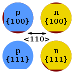
Wafer flats convention, based on Image:Wafer flats convention.PNG Conventional meaning of flats in semiconductor wafers. Red denotes material that has been removed. Wafer orientation is the orientation of the crystallographic plane in which the crystal grew. Wafer type indicated the type of doping.
|
| Dátum | |
| Zdroj |
self-made, Táto W3C-nešpecifikovaná vektorová grafika bola vytvorená pomocou Inkscape . |
| Autor | Twisp |
| Ďalšie verzie | Wafer flats convention.PNG |
Licencovanie
| Ja, držiteľ autorských práv k tomuto dielu, uvoľňujem toto dielo ako voľné dielo (public domain). Toto platí celosvetovo. V niektorých krajinách to zákon neumožňuje; v tom prípade: Udeľujem komukoľvek právo používať toto dielo na ľubovoľné účely, bez akýchkoľvek podmienok ak také podmienky nevyžaduje zákon. |
História súboru
Po kliknutí na dátum/čas uvidíte ako súbor vyzeral vtedy.
| Dátum/Čas | Náhľad | Rozmery | Používateľ | Komentár | |
|---|---|---|---|---|---|
| aktuálna | 21:40, 24. september 2013 | | 150 × 150 (13 KB) | Cepheiden | fixed position of secondary flat Silicon processing for the VLSI era - Vol. 1 - Process technology; S Wolf; RN Tauber - Lattice Press; 1986; ISBN 096167237; p. 23 |
| 00:37, 23. december 2008 |  | 150 × 150 (13 KB) | Inductiveload | Added arrow indication <110> direction and enlarged flats so they can be easily seen | |
| 21:17, 29. február 2008 |  | 150 × 150 (9 KB) | Twisp | ||
| 21:13, 29. február 2008 |  | 150 × 150 (9 KB) | Twisp | ||
| 21:06, 29. február 2008 |  | 150 × 150 (8 KB) | Twisp | ||
| 20:59, 29. február 2008 |  | 150 × 150 (8 KB) | Twisp | ||
| 18:09, 29. február 2008 |  | 150 × 150 (9 KB) | Twisp | {{Information |Description= Wafer flats convention, based on Image:Wafer flats convention.PNG Conventional meaning of ''flats'' in semiconductor wafers. Black denotes material that has been removed. Wafer orientation is |
Použitie súboru
Na tento súbor odkazuje nasledujúca stránka:
Globálne využitie súborov
Nasledovné ďalšie wiki používajú tento súbor:
- Použitie na ca.wikipedia.org
- Použitie na cs.wikipedia.org
- Použitie na de.wikipedia.org
- Použitie na en.wikipedia.org
- Použitie na es.wikipedia.org
- Použitie na et.wikipedia.org
- Použitie na eu.wikipedia.org
- Použitie na fi.wikipedia.org
- Použitie na it.wikipedia.org
- Použitie na it.wikibooks.org
- Použitie na ja.wikipedia.org
- Použitie na ko.wikipedia.org
- Použitie na nl.wikipedia.org
- Použitie na pl.wikipedia.org
- Použitie na ro.wikipedia.org
- Použitie na uk.wikipedia.org
- Použitie na www.wikidata.org